Wednesday, 14 August 2013

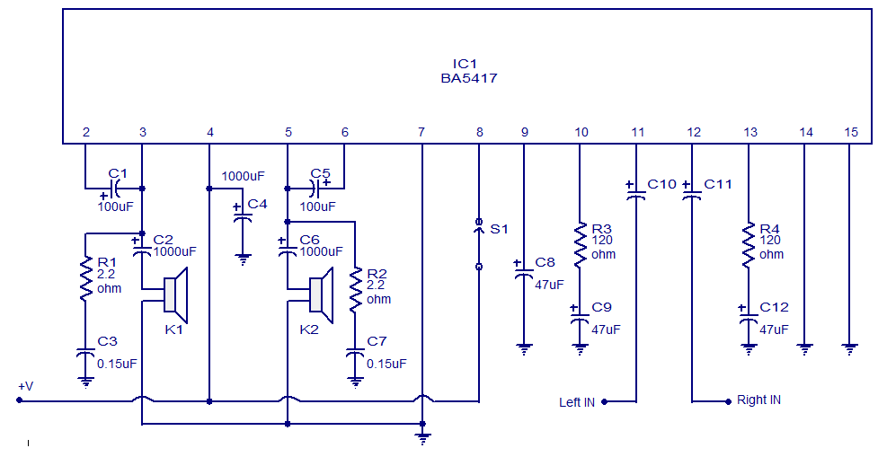
2×5 W Stereo power amplifier circuit based on BA5417.


BA5417 is a stereo amplifier IC with a lot of good features like thermal shut down, standby function, soft clipping, wide operating voltage range etc. The IC can deliver 5W per channel into 4 ohm loud speakers at 12V DC supply voltage. The BA5417 has excellent sound quality and low THD (total harmonic distortion) around 0.1% at F=1kHz; Pout=0.5W.

Description.

Setup and working of this stereo power amplifier circuit is somewhat similar to the BA5406 based stereo amplifier circuit published previously. C10 and C11 are DC decoupling capacitors which block any DC level present in the input signals. C2 and C6 couples the amplifiers left and right power outputs to the corresponding loud speakers. C1 and C5 are bootstrap capacitors. Bootstrapping is a method in which a portion of the amplifiers is taken and applied to the input. The prime objective of bootstrapping is to improve the input impedance. Networks R1,C3 and R2,C7 are meant for improving the high frequency stability of the circuit. C4 is the power supply filter capacitor. S1 is the standby switch. C8 is a filter capacitor. R3 and R4 sets the gain of the left and right channels of the amplifier in conjunction with the 39K internal feedback resistors.

Circuit diagram.

stereo amplifier circuit BA5417
BA5417 stereo amplifier circuit


Notes.

  • Supply voltage range of BA5417 is from 6 to 15V DC.
  • The recommended supply voltage for this circuit is 12V DC.
  • The power supply must be well regulated and filtered.
  • BA5417 requires a heatsink.
  • The circuit can be assembled on a perf board without much degradation in performance.

Few other stereo amplifier circuits that you may like.

BA5406 stereo amplifier circuit : Simple stereo amplifier circuit that can deliver 5 watt per channel sound output into a 4 ohm speaker. Operates from 12V DC and requires very few external components. Suitable for low power car audio applications.
TDA1554 stereo amplifier circuit:  A very popular stereo amplifier design. This amplifier can output 22 watts per channel into 4 ohm loud speakers. This circuit can be also powered from 12V DC. Low distortion and noise.
2×32 watts stereo amplifier circuit : High quality stereo amplifier design using TDA2050 IC. The circuit requires a +/-18V DC dual supply. Power output is 32 watts per channel into 4 ohm speakers.
Stereo amplifier based on TDA4935 : A stereo amplifier design with a lot of great features like over load protection and thermal shut down. The power out put is 2×15 W into 4 ohm speakers. Operating voltage is 24V DC. Potentiometers for controlling the volume is also included in the circuit.
120W stereo amplifier circuit : A powerful stereo amplifier design using LM4780 audio amplifier IC from National Semiconductors. operates from a +/-35V DC dual power supply. 2×60 watt power output into 8 ohm loud speakers. The circuit has good power supply rejection and also there is a built in mute circuitry.
Stereo headphone amplifier


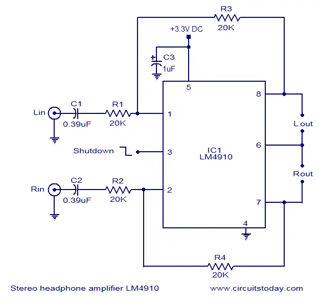
LM4910 stereo headphone amplifier.

LM4910 belonging to the Boomer series of National Semiconductors is an integrated stereo amplifier primarily intended for stereo headphone applications. The IC can be operated from 3.3V ans its can deliver 0.35mW output power into a 32 ohm load. The LM4910 has very low distortion ( less than 1%)   and the shutdown current is less than 1uA. This low shut down current makes it suitable for battery operated applications. The IC is so designed that there is no need of the output coupling capacitors, half supply by-pass capacitors and bootstrap capacitors. Other features of the IC are   turn ON/OFF click elimination, externally programmable gain etc.

Circuit diagram.

Lm4910 headphone amplifier
Stereo headphone amplifier LM4910
Circuit diagram of the LM4910  stereo headphone amplifier is shown above.C1 and C2 are the input DC decoupling capacitors for the left and right input channels. R1 and R2 are the respective input resistors. R3 is the feed back resistor for left channel while R4 is the feed back resistor for the right channel. C3 is the power supply filter capacitor. The feedback resistors also sets the closed loop gain in conjunction with the corresponding input resistors.

Notes.

  • The IC is available only  in SMD packages and care must be taken while soldering.
  • The circuit can be powered from anything between 2.2V to 5V DC.
  • The load can be a 32 ohm headphone.
  • Absolute maximum supply voltage is 6V  and anything above it will destroy the IC.
  • A logic low voltage at the shutdown pins shut downs the IC and a logic high voltage at the same pin activates the IC.

555 Timer as an Astable Multivibrator


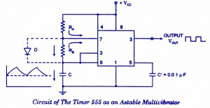
An astable multivibrator, often called a free-running multivibrator, is a rectan­gular-wave generating cir­cuit. Unlike the monostable multivibrator, this circuit does not require any ex­ternal trigger to change the state of the output, hence the name free-running. Before going to make the circuit, make sure your 555 IC is working. For that go through the article: How to test a 555 IC for working An astable multivibrator can be produced by adding resistors and a capacitor to the basic timer IC, as illustrated in figure. The timing during which the output is either high or low is determined by the externally connected two resistors and a capacitor. The details of the astable multivibrator circuit are given below.
555-Astable-Multivibrator
Take a look @ 555 Ic Pin configuration and 555 block diagram before reading further.
Pin 1 is grounded; pins 4 and 8 are shorted and then tied to supply +Vcc, output (VOUT is taken form pin 3; pin 2 and 6 are shorted and the connected to ground through capacitor C, pin 7 is connected to supply + VCCthrough a resistor RA; and between pin 6 and 7 a resistor RB is connected. At pin 5 either a bypass capacitor of 0.01  F is connected or modulation input is applied.

Astable Multivibrator Operation

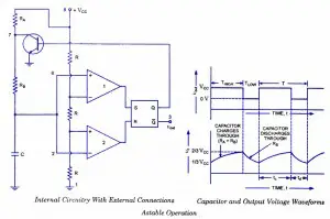
For explaining the operation of the timer 555 as an astable multivibrator, necessary internal circuitry with external connections are shown in figure.
Astable-Multivibrator-Operation
In figure, when Q is low or output VOUT is high, the discharging transistor is cut-­off and the capacitor C begins charging toward VCC through resistances RA and RB. Because of this, the charging time constant is (RA + RB) C. Eventually, the threshold voltage exceeds +2/3 VCC, the comparator 1 has a high output and triggers the flip-flop so that its Q is high and the timer output is low. With Q high, the discharge transistor saturates and pin 7 grounds so that the capacitor C discharges through resistance RB with a discharging time constant RB C. With the discharging of capacitor, trigger voltage at inverting input of comparator 2 decreases. When it drops below 1/3VCC, the output of comparator 2 goes high and this reset the flip-flop so that Q is low and the timer output is high. This proves the auto-transition in output from low to high and then to low as, illustrated in fig ures. Thus the cycle repeats.

Astable Multivibrator using 555 IC -Design method

The time during which the capacitor C charges from 1/3 VCC to 2/3 VCC is equal to the time the output is high and is given as tc or THIGH = 0.693 (RA + RB) C, which is proved below.
Voltage across the capacitor at any instant during charging period is given as,vc=VCC(1-et/RC)
The time taken by the capacitor to charge from 0 to +1/3 VCC
1/3 VCC = VCC (1-et/RC)
The time taken by the capacitor to charge from 0 to +2/3 VCC
or t2 = RC log3 = 1.0986 RC
So the time taken by the capacitor to charge from +1/3 VCC to +2/3 VCC
tc = (t2 – t1) =  (10986 – 0.405) RC = 0.693 RC
Substituting R = (RA + RB) in above equation we have
THIGH = t= 0.693 (RA + RB) C
where RA and RB are in ohms and C is in farads.
The time during which the capacitor discharges from +2/3 VCC to +1/3 VCC is equal to
the time the output is low and is given as
td or  TL0W = 0.693 RB C where RB is in ohms and C is in farads The above equation is worked out as follows: Voltage across the capacitor at any instant during discharging period is given as
vc = 2/3 VCC e- td/ RBC
Substituting vc = 1/3 VCC and t = td in above equation we have
+1/3 VCC = +2/3 VCC e- td/ RBC
Or  td = 0.693 RBC
Overall period of oscillations, T = THIGH + TLOW = 0.693 (RA+ 2RB) C , The frequency of oscillations being the reciprocal of the overall period  of oscillations T is given as
f = 1/T = 1.44/ (RA+ 2RB)C
Equation indicates that the frequency of oscillation / is independent of the collector supply voltage +VCC.
Often the term duty cycle is used in conjunction with the astable multivibrator.
The duty cycle, the ratio of the time tc during which the output is high to the total time period T is given as
% duty cycle, D = t/ T * 100 = (RA + RB) / (RA + 2RB) * 100
From the above equation it is obvious that square wave (50 % duty cycle) output can not be obtained unless RA is made zero. However, there is a danger in shorting resistance RA to zero. With RA = 0 ohm, terminal 7 is directly connected to + VCC. During the discharging of capacitor through RB and transistor, an extra current will be supplied to the transistor from VCC through a short between pin 7 and +VCC. It may damage the transistor and hence the timer.
However, a symmetrical square wave can be obtained if a diode is connected across resistor RB, as illustrated in dotted lines in figure. The capacitor C charges through RA and diode D to approximately + 2/3VCC and discharges through resistor RB and terminal 7 (transistor) until the capacitor voltage drops to 1/3 VCC. Then the cycle is repeated. To obtain a square wave output, RA must be a combination of a fixed resistor R and a pot, so that the pot can be adjusted to give the exact square wave.
Although the timer 555 has been used in a wide variety of often unique applications it is very hard on its power supply lines, requiring quite a bit of current, and injecting many noise transients. This noise will often be coupled into adjacent ICs falsely triggering them. The 7555 is a CMOS version of the 555. Its quiescent current requirements are considerably lower than that of 555, and the 7555 does not contaminate the power supply lines. It is pin compatible with the 555. So this CMOS version of the 555 should be the first choice when a 555 timer IC is to be used.

555 Timer as Monostable Multivibrator


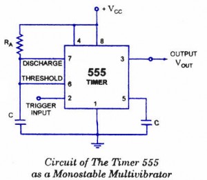
A monostable multivibrator (MMV) often called a one-shot multivibrator, is a pulse generator circuit in which the duration of the pulse is determined by the R-C network,connected externally to the 555 timer. In such a vibrator, one state of output is stable while the other is quasi-stable (unstable). For auto-triggering of output from quasi-stable state to stable state energy is stored by an externally connected capaci­tor C to a reference level. The time taken in storage determines the pulse width. The transition of output from stable state to quasi-stable state is accom­plished by external triggering. The schematic of a 555 timer in monostable mode of operation is shown in figure.
555-timer-monostable-multivibrator

Monostable Multivibrator Circuit details

Pin 1 is grounded. Trigger input is applied to pin 2. In quiescent condition of output this input is kept at + VCC. To obtain transition of output from stable state to quasi-stable state, a negative-going pulse of narrow width (a width smaller than expected pulse width of output waveform)  and  amplitude of greater than + 2/3 VCC is applied to pin 2. Output is taken from pin 3. Pin 4 is usually connected to + VCC to avoid accidental reset. Pin 5 is grounded through a 0.01 u F capacitor to avoid noise problem. Pin 6 (threshold) is shorted to pin 7. A resistor RA is connected between pins 6 and 8. At pins 7 a discharge capacitor is connected while pin 8 is connected to supply VCC.

555 IC Monostable Multivibrator Operation.

555 monostable-multivibrator-operation
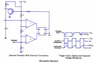
For explain­ing the operation of timer 555 as a monostable multivibrator, necessary in­ternal circuitry with external connections are shown in figure.

The operation of the circuit is ex­plained below:

Initially, when the output at pin 3 is low i.e. the circuit is in a stable state, the transistor is on and capacitor- C is shorted to ground. When a negative pulse is applied to pin 2, the trigger input falls below +1/3 VCC, the output of comparator goes high which resets the flip-flop and consequently the transistor turns off and the output at pin 3 goes high. This is the transition of the output from stable to quasi-stable state, as shown in figure. As the discharge transistor is cut­off, the capacitor C begins charging toward +VCC through resistance RA with a time constant equal to RAC. When the increasing capacitor voltage becomes slightly greater than +2/3 VCC, the output of comparator 1 goes high, which sets the flip-flop. The transistor goes to saturation, thereby discharging the capacitor C and the output of the timer goes low, as illustrated in figure.
Thus the output returns back to stable state from quasi-stable state.
The output of the Monostable Multivibrator remains low until a trigger pulse is again applied. Then the cycle repeats. Trigger input, output voltage and capacitor voltage waveforms are shown in figure.

Monostable Multivibrator Design Using 555 timer IC

The capacitor C has to charge through resistance RA. The larger the time constant RAC, the longer it takes for the capacitor voltage to reach +2/3VCC.
In other words, the RC time constant controls the width of the output pulse. The time during which the timer output remains high is given as
tp = 1.0986 RAC
where RA is in ohms and C is in farads. The above relation is derived as below. Voltage across the capacitor at any instant during charging period is given as
v= VCC (1- e-t/RAC)
Substituting vc = 2/3 VCC in above equation we get the time taken by the capacitor to charge from 0 to +2/3VCC.
So +2/3VCC. = VCC. (1 – e-t/RAC)   or   t – RAC loge 3 = 1.0986 RAC
So pulse width, tP = 1.0986 RAC s 1.1 RAC
The pulse width of the circuit may range from micro-seconds to many seconds. This circuit is widely used in industry for many different timing applications.

555 Timer Oscillator


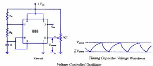
555-timer-voltage-controlled-oscillator
The circuit is sometimes called a voltage-to-frequency converter because the output frequency can be changed by changing the input voltage.
As discussed in previous blog posts, pin 5 terminal is voltage control terminal and its function is  to control the threshold and trigger levels. Normally, the control voltage is ++2/3VCC because of the internal voltage divider. However, an external voltage can be applied to this terminal directly or through a pot, as illustrated in figure, and by adjusting the pot, control voltage can be varied. Voltage across the timing capacitor is depicted in figure, which varies between +Vcontrol and ½ VcontrolIf control voltage is increased, the capacitor takes a longer to charge and discharge; the frequency, therefore, decreases. Thus the fre­quency can be changed by changing the control volt­age. Incidentally, the control voltage may be made available through a pot, or it may be output of a transistor circuit, op-amp, or some other device.

Ramp Generator Circuit-using 555 Timer IC


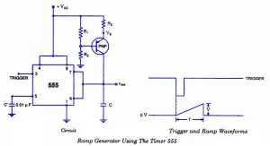
We know that if a capacitor is charged from a voltage source through a resistor, an exponential waveform is produced while charging of a capaci­tor from a constant current source produces a ramp. This is the idea behind the circuit. The circuit of a ramp generator using timer 555 is shown in figure. Here the resistor of previ­ous circuits is replaced by a PNP transistor that produces a constant charging current.
Ramp Generator Circuit
Charging current produced by PNP constant current source is
i= Vcc-V/ RE
where V= R/ (R1 + R2) * VCC + VBE
When a trigger starts the monostable multivibrator timer 555 as shown in figure, the PNP current source forces a constant charging into the capacitor C. The voltage across the capacitor is, therefore, a ramp as illustrated in the figure. The slope of the ramp is given as
Slope, s = I/C

Police siren using NE555


Description.
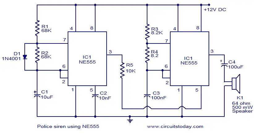
A lot of electronic circuits using NE555 timer IC are already published here and this is just another one.Here is the circuit diagram of a police siren based on NE55 timer IC. The circuit uses two NE555 timers ICs and each of them are wired as astable multivibrators.The circuit can be powered from anything between 6 to 15V DC and is fairly loud.By connecting an additional power amplifier at the output you can further increase the loudness.
IC1 is wired as a slow astable multivibrator operating at around 20Hz @ 50% duty cycle and IC2 is wired as fast astable multivibrator operating at around 600Hz.The output of first astable mutivibrator is connected to the control voltage input (pin5) of IC2. This makes the output of IC2 modulated by the output frequency of IC1, giving a siren effect. In simple words, the output frequency of IC2 is controlled by the output of IC1.
Circuit diagram.
police-siren-using-NE555
Notes.
  • The circuit can be assembled on a Perf board.
  • I used 12V DC for powering the circuit.
  • Instead of using two NE55 timer ICs, you can also use a single NE556 timer.
  • NE556 is nothing but two NE555 ICs in one package.
  • Refer the datasheets of NE555 and NE556 to have a clear idea.
  • Speaker can be a 64ohm, 500mW one.